Industrial Femtosecond Lasers FemtoLux
Industrial Femtosecond Lasers
FemtoLux is designed from the get-go for maximum reliability, seamless integration and non-stop 24/7/365 zero maintenance operation with innovative ”dry” cooling. Wide range of options enable to tailor this ultrafast laser for desired material processing tasks.

Features
- At 1030 nm
50 W typical max output power
> 300 µJ typical max output energy - At 515 nm
20 W typical max output power
> 50 µJ typical max output energy - At 343 nm
10 W typical max output power
> 25 µJ typical max output energy - Up to 1 mJ for FemtoLux HE
- Up to 2 mJ in a burst mode
- < 400 fs – 1 ps
- Pulse duration extension up to 1 ns
- Single shot – up to 4 MHz (AOM controlled)
- MHz, GHz, MHz+GHz burst modes
- Pulse-on-demand (PoD), with jitter as low as 20 ns (peak-to-peak)
- < 0.5% RMS power long term stability over 100 hours
- M² < 1.2
- Beam ellipticity > 0.85
- Zero maintenance
- Dry cooling (no water used)
- PSU and cooling unit integrated into single 4U rack housing
- Easy and quick installation
- Compatible with galvo and Polygon scanners as well as PSO controllers
A reliable & versatile tool for micromachining
Designed from the get-go for maximum reliability, seamless integration and non-stop 24/7/365 zero maintenance operation with innovative ”dry” cooling.
The FemtoLux femtosecond laser has a tunable pulse duration from <400 fs to 1 ps and can operate in a broad AOM controlled range of pulse repetition rates from a single shot to 4 MHz.
The maximum pulse energy is 1 mJ operating with single pulses and can reach even up to 2 mJ in burst mode, ensuring higher ablation rates and processing throughput for different materials.
The FemtoLux beam parameters will meet the requirements of the most demanding materials and micro-machining applications.
Innovative laser control electronics ensure simple control of the FemtoLux laser by external controllers that could run on different platforms, be it Windows, Linux or others using REST API commands.
This makes easy integration and reduces the time and human resources required to integrate this laser into any laser micromachining equipment.

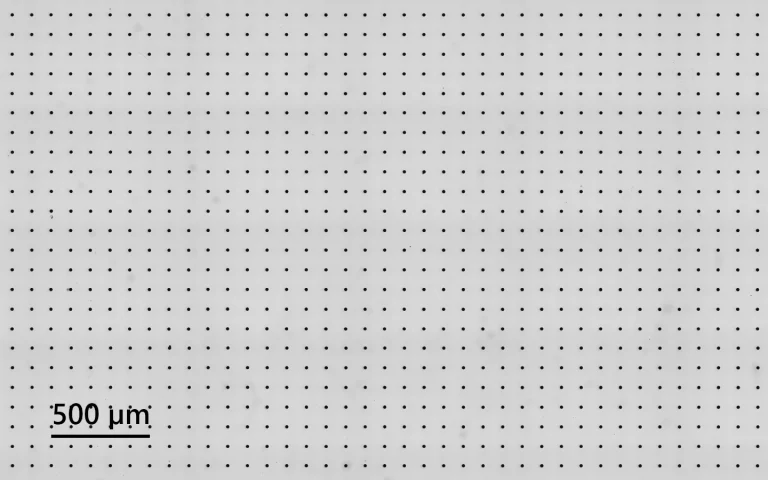
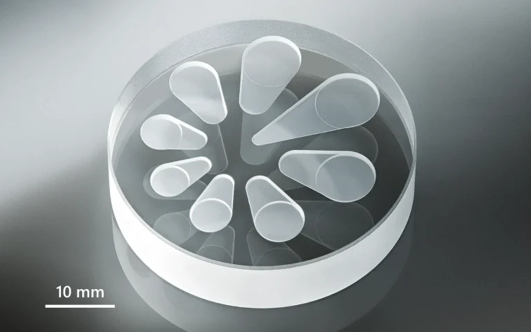
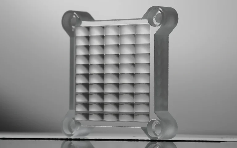
Material processing examples made with FemtoLux laser.
Courtesy of FTMC and Femtika.
Seamless user experience
- Easy integration – remote control using REST API via RS232 and LAN.
- Reduced integration time – demo electronics is available for laser control programming in advance.
- Easy and quick installation – no water, fully disconnectable laser head. Can be installed by the end-user.
- Easy troubleshooting – integrated detectors and constant system status logging.
- No periodic maintenance required.
“Dry“ Cooling
Direct refrigerant cooling is industry-proven thermal-management approach with a long history in everyday technologies such as domestic refrigeration and automotive climate control. Unlike conventional liquid cooling, it operates without pumped water circuits, relying instead on direct refrigerant-based heat transfer.
Benefits
- Military-grade reliability 90 000 hours MTBF
- No maintenance
- 50 % lower power consumption compared to water cooling equipment
- Easy and simple installation
- Increased stability due to precise temperature control across a wide range of operating conditions
- “Greenest” cooling technology
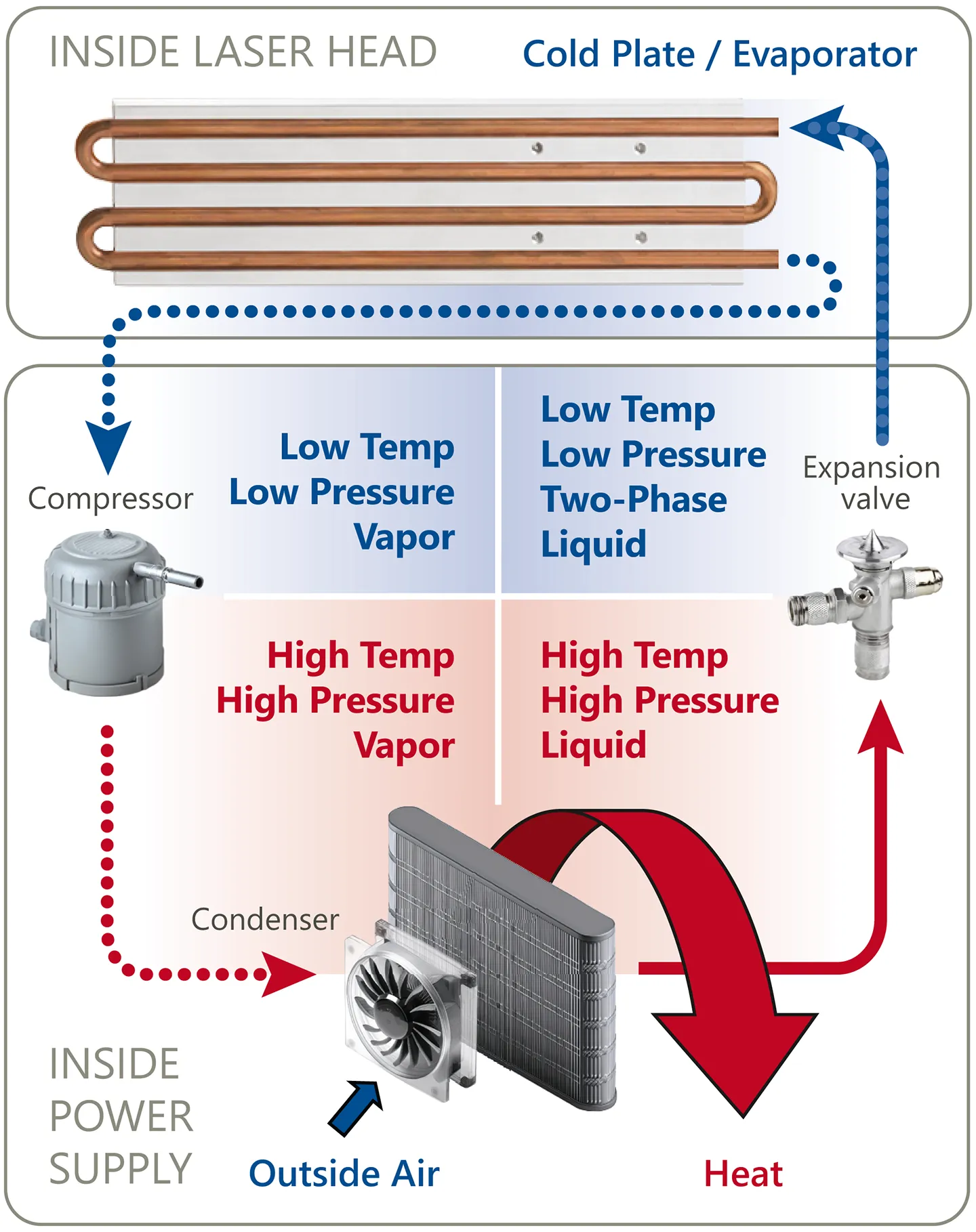
How DRC Works
At its core, DRC eliminates the inherent reliability limitations of water-based cooling loops. Rather than circulating liquid coolant through pumps, hoses, and reservoirs, refrigerant is delivered directly to a cold plate that is in contact to the laser head.
The FemtoLux cooling architecture comprises four key elements: a compressor, condenser, expansion valve, and evaporator. High-pressure refrigerant is circulating through the expansion valve, which is mounted directly on the cooling plate. As the refrigerant expands, it enters the plate as a low-temperature, low-pressure liquid. While flowing through the plate, it absorbs heat from the laser head and undergoes a controlled phase change into vapor. This vapor is then compressed and routed through the condenser, where heat is released to the surrounding environment and the refrigerant returns to liquid form.
The closed refrigerant circuit provides exceptional integration flexibility. The compressor and condenser are housed within the power supply unit, while the cooling plate and expansion valve are connected via three‑meter armored flexible lines. This arrangement allows the laser head to be installed inside material processing workstations or mounted on moving stages. A variable-speed compressor continuously adjusts cooling output to match real-time thermal demand, preventing temperature fluctuations that can affect laser performance.
DRC layout.
Courtesy of Aspen Systems Inc.
DRC compressor picture.
Courtesy of Aspen Systems Inc.
DRC module used in FemtoLux lasers.
A cooling plate is attached to the laser on one side of the design (above). On the other, a compressor with auxiliary electronics is installed into the laser power supply unit.
Straightforward Installation and Maintenance-Free Operation
For ease of integration, the cooling plate can be detached from the laser head during system assembly. Flexible refrigerant lines allow the laser head to be positioned independently of the compressor unit, simplifying mechanical integration.
Because the refrigerant loop is hermetically sealed at the factory, routine maintenance associated with water-based systems – such as refilling, filter changes, or system flushing – is eliminated entirely.
For system integrators, dry cooling represents a substantial step forward. By removing the constraints of water and air cooling, DRC simplifies system design while enabling compact layouts. The streamlined cold-plate interface reduces installation complexity, and the compact power supply unit supports straightforward system integration.
The absence of pumps and reservoirs keeps system dimensions small. The compressor is up to 10 times smaller and lighter than conventional designs. The FemtoLux laser head with integrated cooling plate weighs 32 kg, while the power supply unit – including compressor and condenser – adds only 15 kg.

The cooling plate is detachable from the laser head.
The cooling plate cover.
Precision Temperature Control and Energy Efficiency
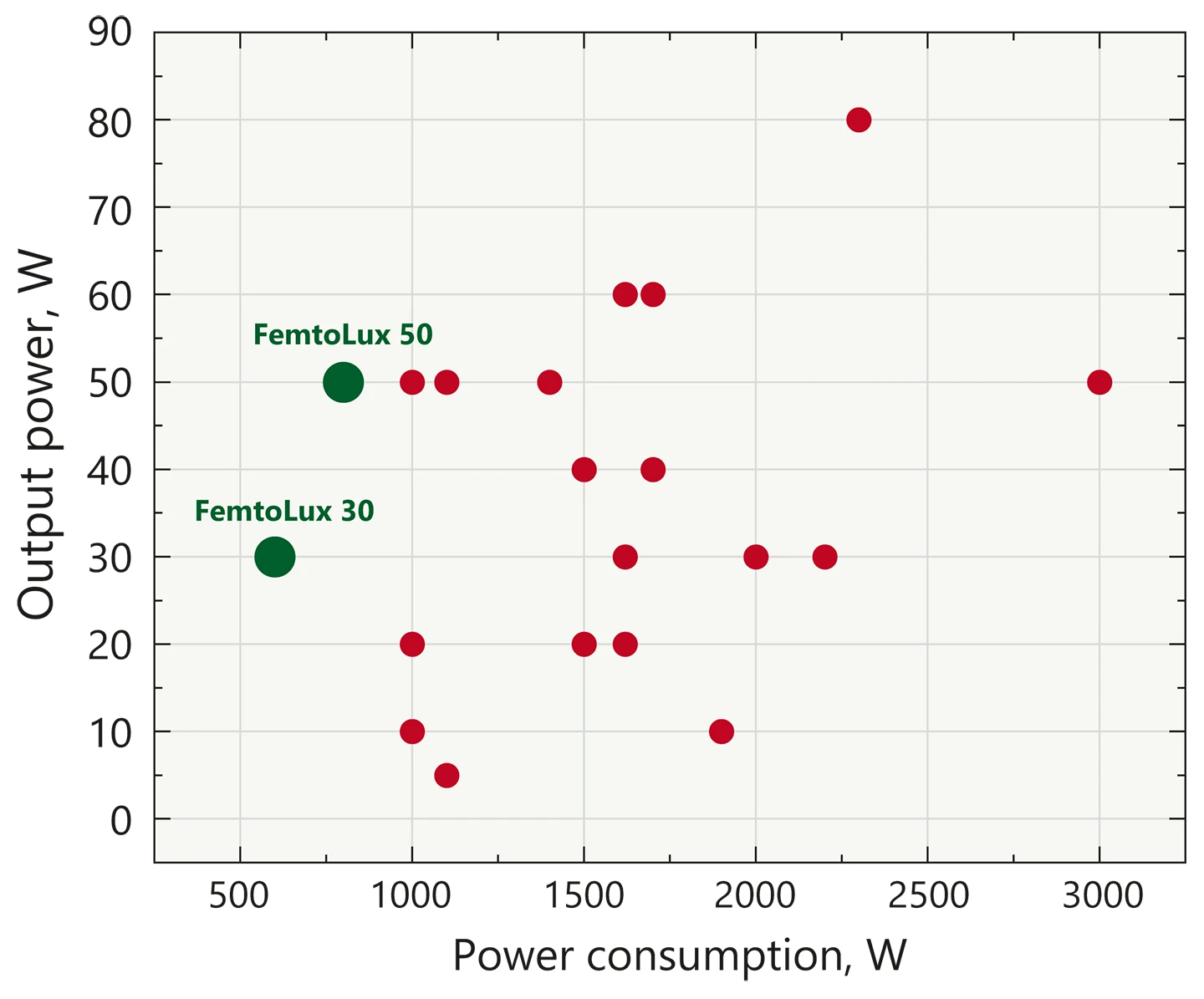
FemtoLux 30 and 50 power consumption and output power comparison versus other ultrafast lasers manufacturers.
Direct refrigerant cooling delivers approximately 50% higher energy efficiency than water-cooled solutions, while maintaining highly uniform cold-plate temperatures through phase-change heat transfer. Comparative testing has shown that DRC systems consume roughly half the electrical power of traditional liquid chillers under identical operating conditions.
Thermal regulation is both precise and responsive. The variable-speed compressor adapts continuously to changing heat loads, maintaining laser operating temperature within ±0.1 °C across the full performance range.
FemtoLux lasers use a low–global-warming-potential (GWP) refrigerant approved for laboratory operation and transport. Compared to alternative cooling methods, DRC consumes about half the power of chiller-based systems and up to eight times less than thermoelectric cooling solutions. Unlike air cooling, DRC can operate below ambient temperature or hold a tightly defined thermal setpoint.
Proven Reliability from Military to Industry
This cooling approach has been deployed by Aspen Systems for more than 15 years in demanding defense applications where size, weight, efficiency, and reliability are critical. These include military communications systems, high-power directed-energy platforms on armored vehicles, transport enclosures, ships, and helicopters.
The technology demonstrates a mean time between failures (MTBF) exceeding 90,000 hours, enabling continuous operation for more than a decade. In long-term testing, FemtoLux lasers have demonstrated stable operation beyond 25,000 hours. Compressor service life typically surpasses that of water-chiller pumps by a factor of three to five, further enhancing system reliability.
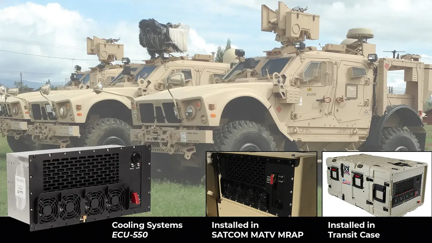
Aspen Systems’ refrigeration systems, as used in military applications.
Courtesy of Aspen Systems Inc.
Dry cooling technology developed by EKSPLA engineers is featured as the cover story in the November, 2025 issue of Photonics Spectra, the industry’s leading magazine with the largest worldwide circulation in lasers, optics, and photonics.
Benefits
- Jitter lower than 20 ns ensures consistent and equidistant pulse spacing for high-speed micromachining
- Adjustable repetition rate for processing complex geometries
- Faster processing speeds, increased productivity
How Pulse‑on‑Demand Works
PoD feature enables the laser to fire a pulse only when required, rather than at a constant rate, enabling precise control over the laser’s output and resulting in higher efficiency, accuracy and quality.
This capability is especially valuable in various micromachining applications where a high processing speed, constant energy, and accuracy are essential. To follow complex curvature at high speed and to maintain equidistant spacing it is necessary to ensure that the repetition rate of the pulses is adjusted. To achieve these requirements, it is necessary to ensure that the repetition rate of the pulses is adjusted to follow complex curvature at high speed and to maintain equidistant spacing. One may try to use position based laser triggering but, due to laser system limitations, the jitter will be from several μs to tens of μs, which will result in random spacing of the pulses.
On the other hand, the usage of time based laser triggering results in overheat areas, due to excessive overlap of pulses. The FemtoLux laser has the pulse-on-demand feature with jitter as low as 20 ns (peak-to-peak), and it can therefore tackle all the challenges and maximize process efficiency, precision and quality at high speed.
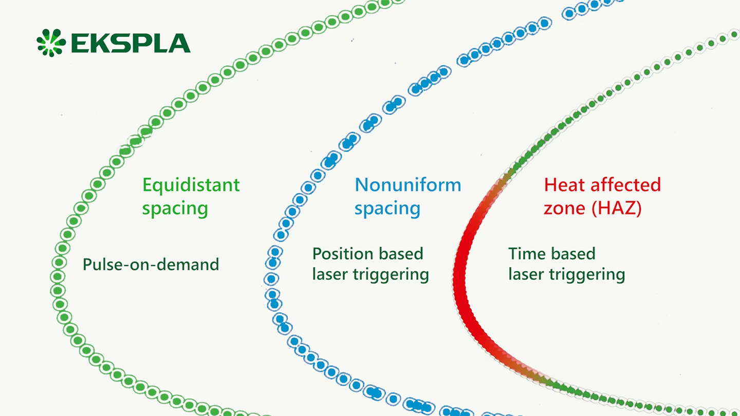
Traditional laser triggering techniques struggle to maintain equally spaced pulses at high speeds (Fig.1, 2). Pulse-on-demand feature tackles this challenge and enables high-speed micromachining (Fig. 3).

Fig. 1. Time based laser triggering.
Complex shape scanned with time based laser triggering mode with a pulse repetition of 200 kHz and scanning speed of 6 m/s. The scanning started from the top right to the bottom right area. Overlapping pulses result in an overheated area.

Fig. 2. Position based laser triggering.
Complex shape scanned with position based laser triggering mode with a pitch of 30 μm and scanning speed of 6 m/s. The scanning started from the top right to the bottom right area. Jitter of tens of μs results in random pulse spacing.

Fig. 3. Pulse-on-demand (PoD).
Complex shape scanned with pulse-on-demand (PoD) and position based laser triggering mode with a pitch of 30 μm and scanning speed of 6 m/s. The scanning started from the top right to the bottom right area. PoD feature preserves equidistant pulse spacing at high speeds.
Benefits
- Any desired intra-burst PRR can be achieved independently from the initial PRR of the master oscillator
- Identical pulse separation inside the GHz bursts is maintained
- Short- and long-burst formation modes can be provided.
– A short burst is up to about 10 ns burst width (from 2 to tens of pulses in the GHz burst).
– A long burst is from ~20 ns up to a few hundred ns in burst width (from tens to thousands of pulses in the GHz burst) - MHz+GHz burst mode
- An adjustable amplitude envelope of the GHz bursts is provided
- No pre/post pulses in GHz burst. Pure GHz bursts
- Ultrashort pulse duration is maintained inside the bursts
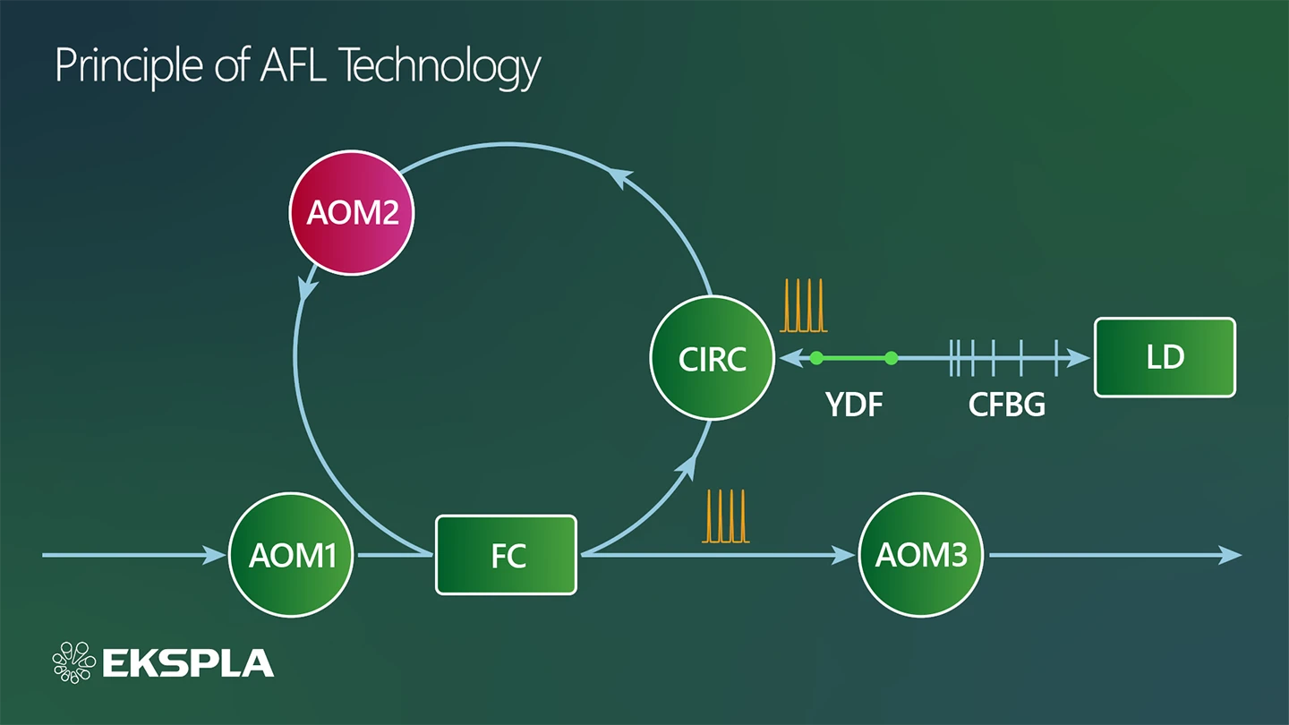
Patent-Pending Method
The Femtolux laser can operate in the single-pulse mode, MHz burst mode, GHz burst mode, and MHz + GHz burst mode.
The burst formation technique based on the use of the AFL is a very versatile method as it allows to overcome many limitations encountered by other fiber- and/or solid-state-based techniques.
A new versatile patent-pending method to form ultra-high repetition rate bursts of ultrashort laser pulses. The developed method is based on the use of an all-in-fiber active fiber loop (AFL). A detailed description of the invention can be found on:
- Tadas Bartulevičius, Mykolas Lipnickas, Virginija Petrauskienė, Karolis Madeikis, and Andrejus Michailovas, (2022), “30 W-average-power femtosecond NIR laser operating in a flexible GHz‑burst-regime,” Opt. Express 30, 36849-36862. DOI: 10.1364/OE.472907.
- Andrejus Michailovas, and Tadas Bartulevičius. 2021 Int. patent application published under the Patent Cooperation Treaty (PCT) WO2021059003A1.
Short GHz burst
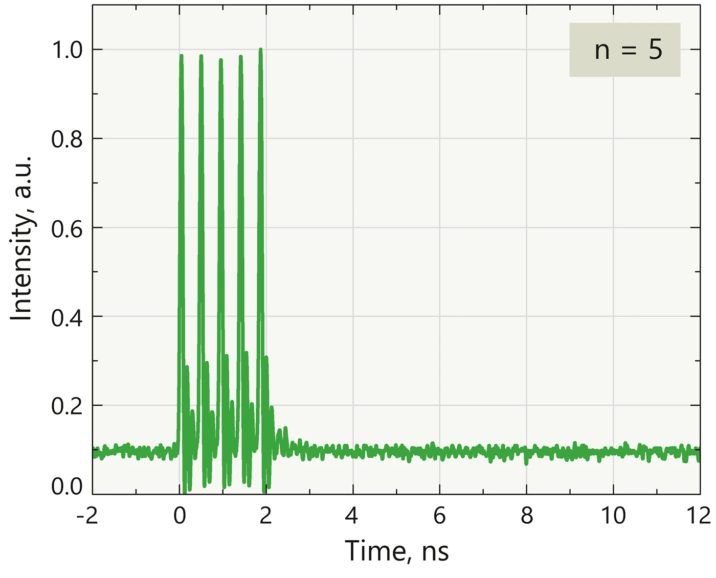
Short GHz burst.
Measured 2.2 GHz intra-burst PRR burst of pulses containing a different number of pulses of equal amplitudes at 31.5 W average output power.
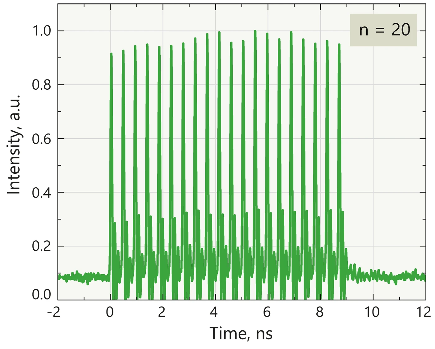
Short GHz burst.
Measured 2.2 GHz intra-burst PRR burst of pulses containing a different number of pulses of equal amplitudes at 31.5 W average output power.
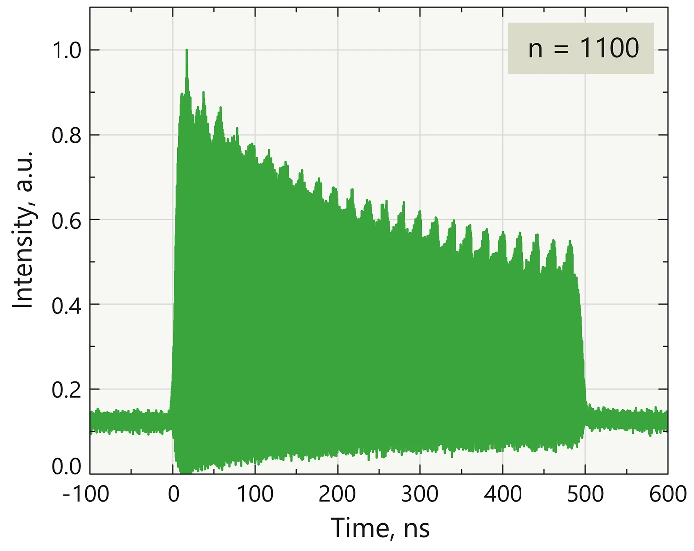
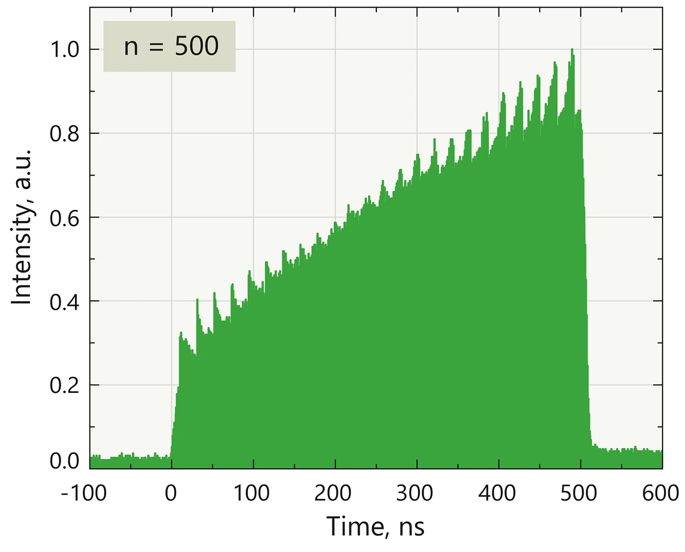
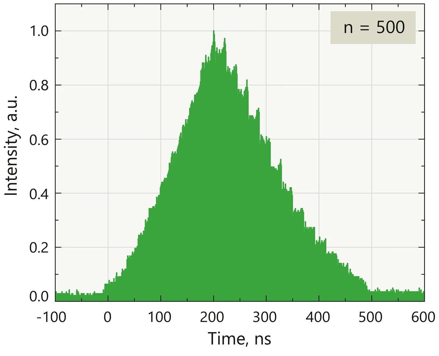
Long GHz burst
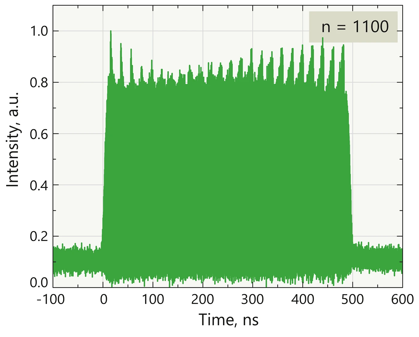
Long GHz burst.
Measured 2.2 GHz pre-shaped bursts of 1100 pulses at 233 kHz burst repetition rate for the desired rectangular-like burst shape.
Long GHz burst.
Measured 2.2 GHz non-pre-shaped bursts of 1100 pulses at 233 kHz burst repetition rate.
Long GHz burst.
Measured 2.2 GHz pre-shaped bursts of 500 pulses at 233 kHz burst repetition rate for the desired rising burst shape.
Long GHz burst.
Measured 2.2 GHz pre-shaped bursts of 500 pulses at 233 kHz burst repetition rate for the desired triangle burst shape.
MHz + GHz burst mode
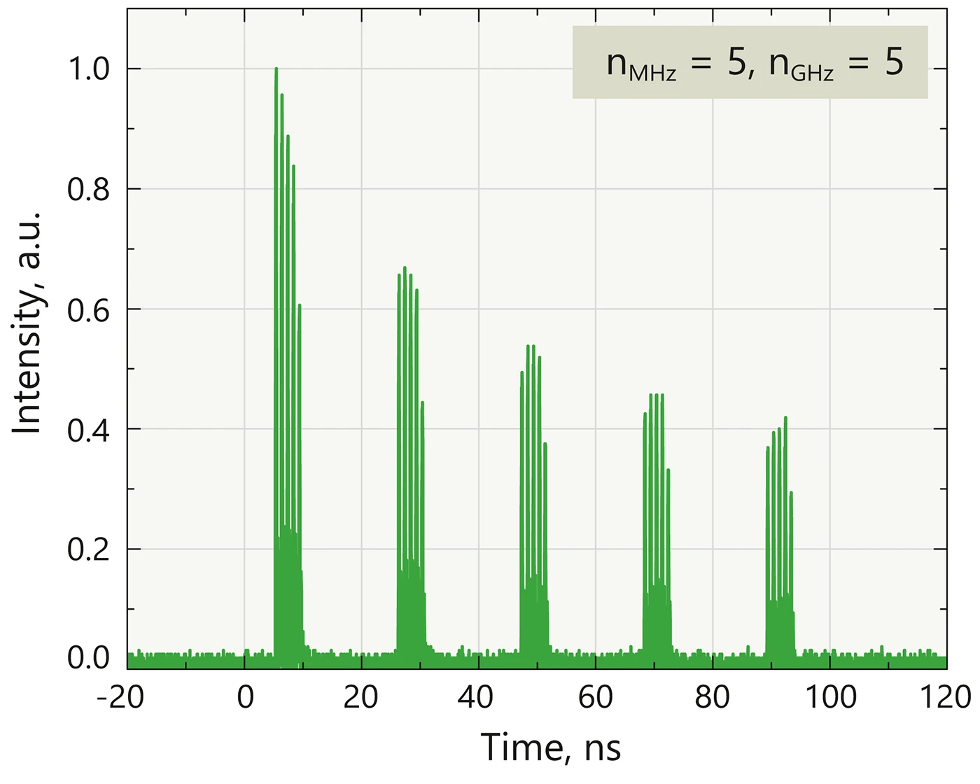
MHz + GHz burst mode.
Measured 5 bursts of 50 MHz burst repetition rate containing 5 pulses of 2.5 GHz intra-burst PRR.
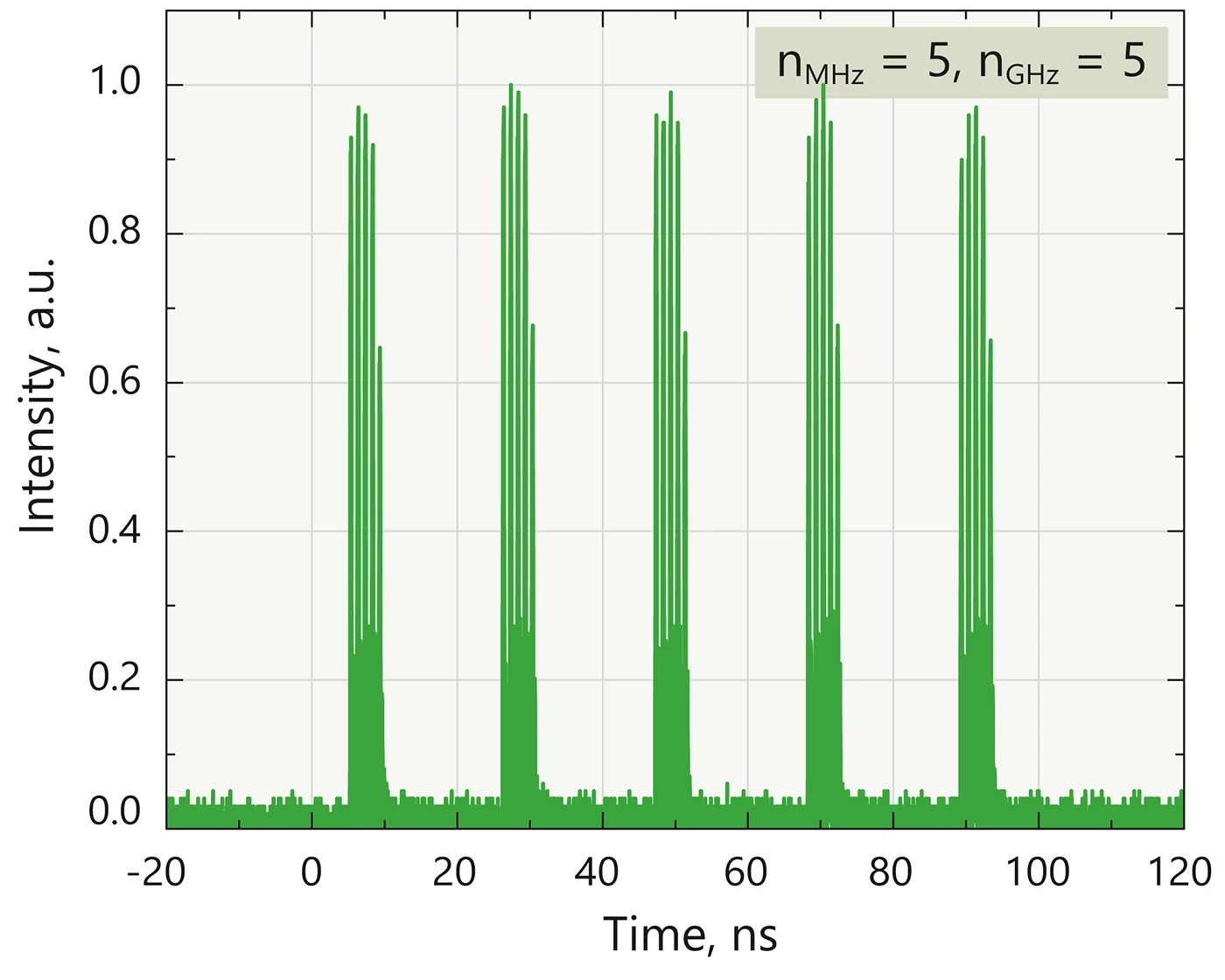
MHz + GHz burst mode.
Measured rectangular shape 5 bursts of 50 MHz burst repetition rate containing 5 pulses of 2.5 GHz intra-burst PRR.
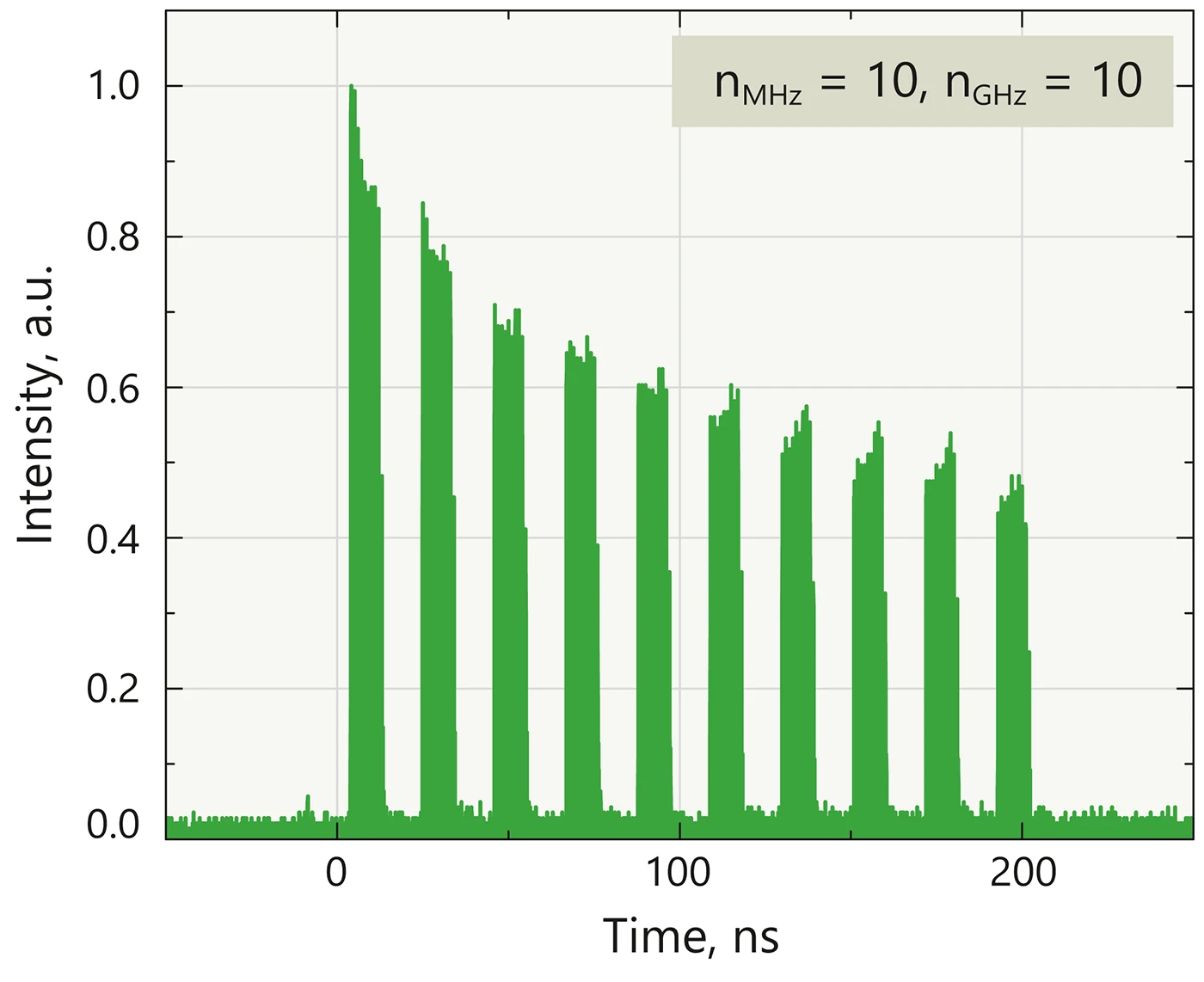
MHz + GHz burst mode.
Measured 10 bursts of 50 MHz burst repetition rate containing 10 pulses of 2.5 GHz intra-burst PRR.
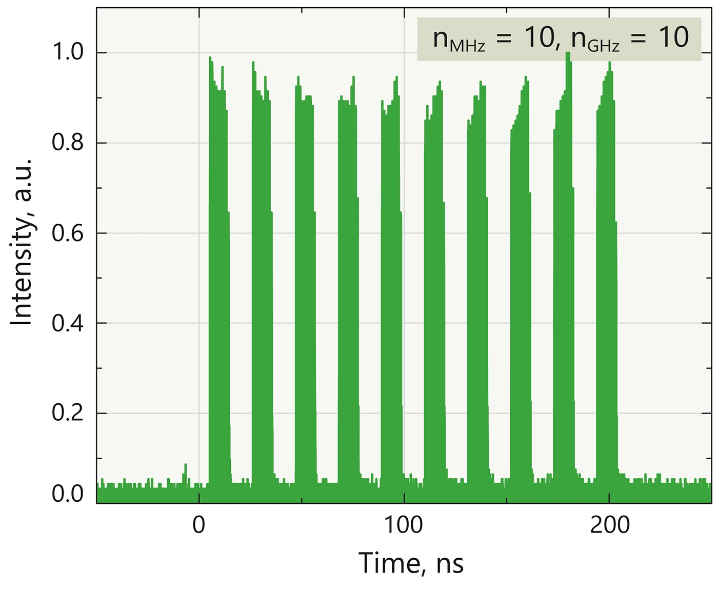
MHz + GHz burst mode.
Measured rectangular shape 10 bursts of 50 MHz burst repetition rate containing 10 pulses of 2.5 GHz intra-burst PRR.
Specifications
| Main specifications 1) | ||
| Laser Pulse Repetition Rate (PRR) | up to 500 kHz | |
| Intra-burst pulse repetition rate 2) | 2 ± 0.25 GHz | |
| GHz burst mode | short | long |
| GHz burst length | 0.5 – 10 ns | 20 – 500 ns |
| Number of pulses 3) | 2 – 20 | 40 – 1000 |
| Shape | square, rising, falling | falling, pre-shaped 3) |
| MHz + GHz Burst Mode | ||
| Number of pulses in MHz burst | 2 – 10 | |
| Number of pulses in GHz burst 4) | 2 – 20 | |
- Due to continuous improvement, all specifications are subject to change without notice. Parameters marked typical are not specifications. They are indications of typical performance and will vary with each unit we manufacture. All parameters are specified for a shortest pulse duration.
- Custom intra-pulse PRR is available upon a request.
- Depends on the intra-pulse PRR.
- For more information, please inquire sales@ekspla.com.
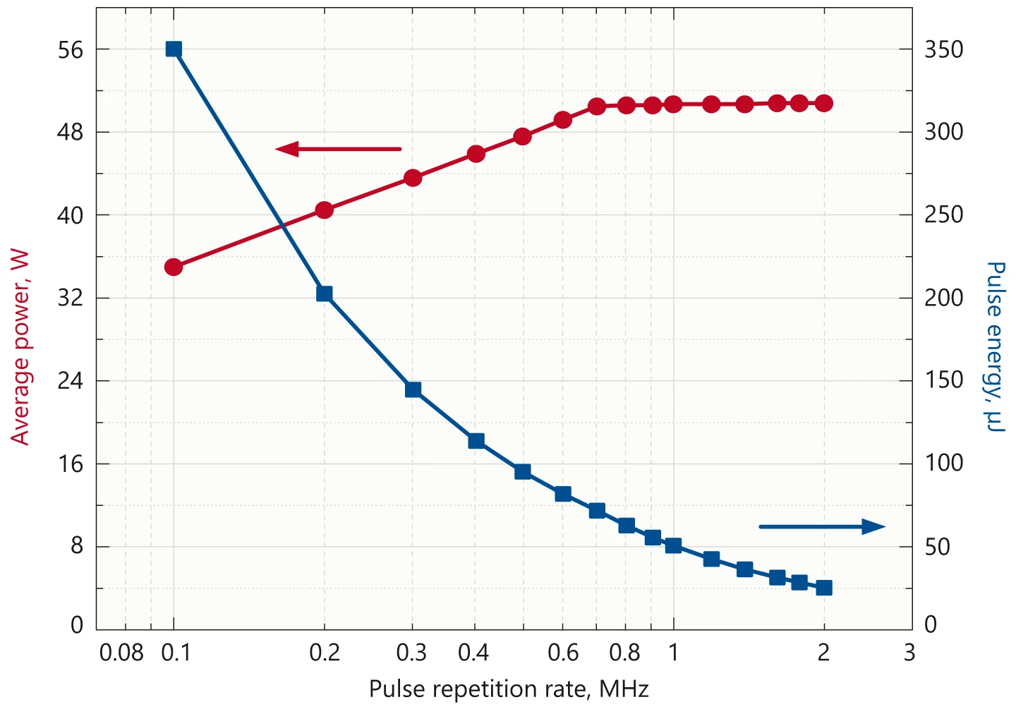
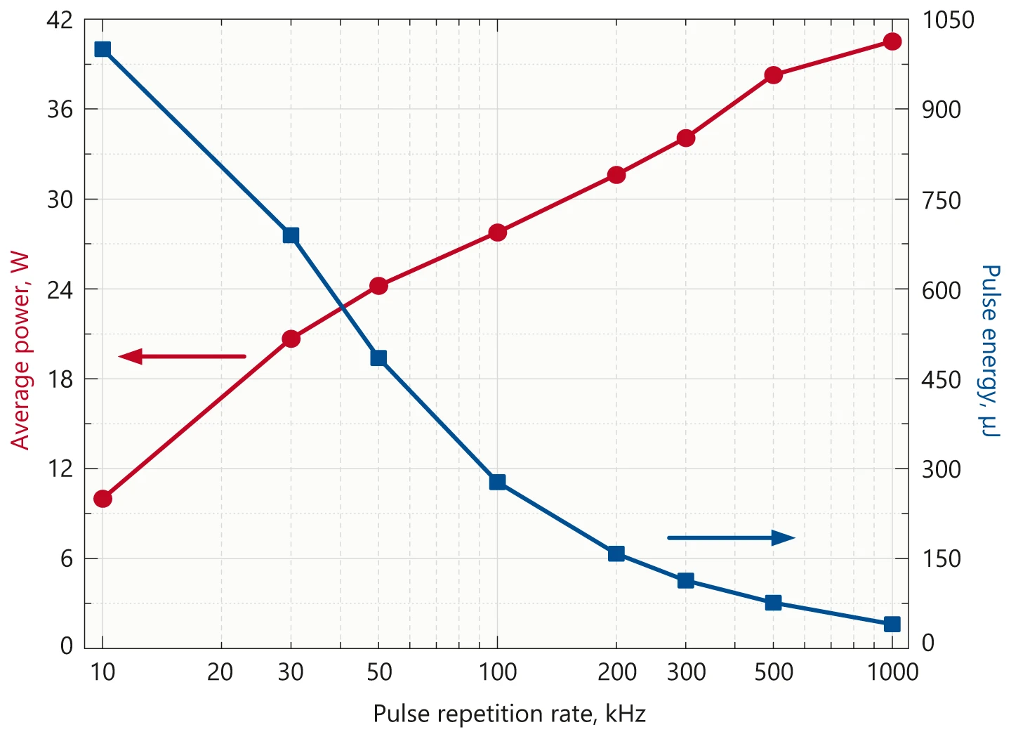
Typical dependence of output power and pulse energy of FemtoLux 50 laser at 1030 nm on pulse repetition rate.
Typical dependence of output power and pulse energy of FemtoLux 50 laser at 515 nm on pulse repetition rate.
Typical dependence of output power and pulse energy of FemtoLux 50 laser at 343 nm on pulse repetition rate.
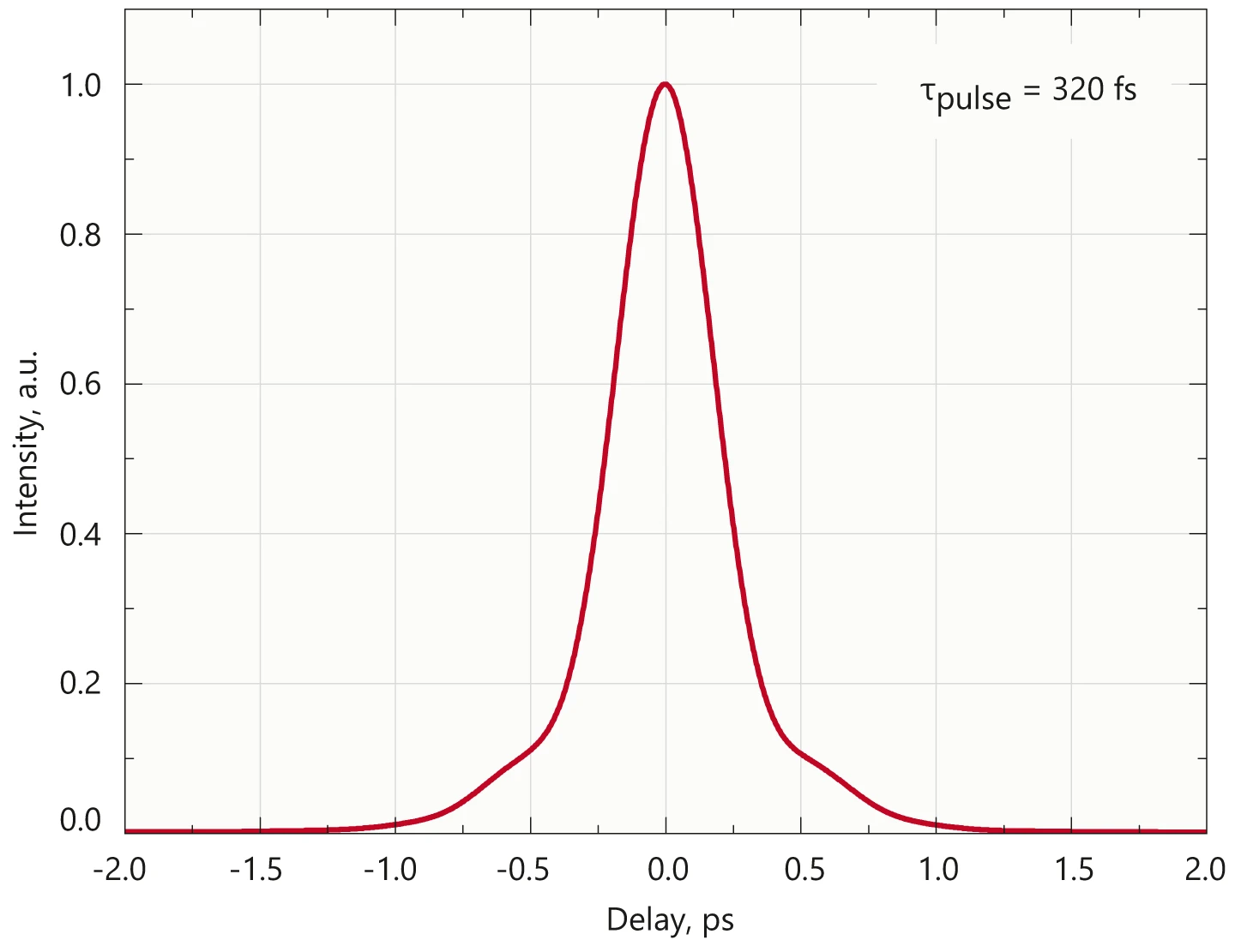
Typical FemtoLux 50 laser output pulse autocorrelation function at 1030 nm @ 1 MHz.
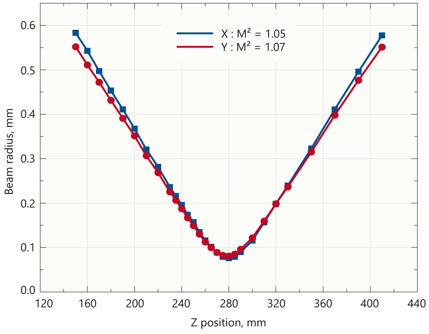
Typical M² measurement of FemtoLux 50 laser at 1030 nm.
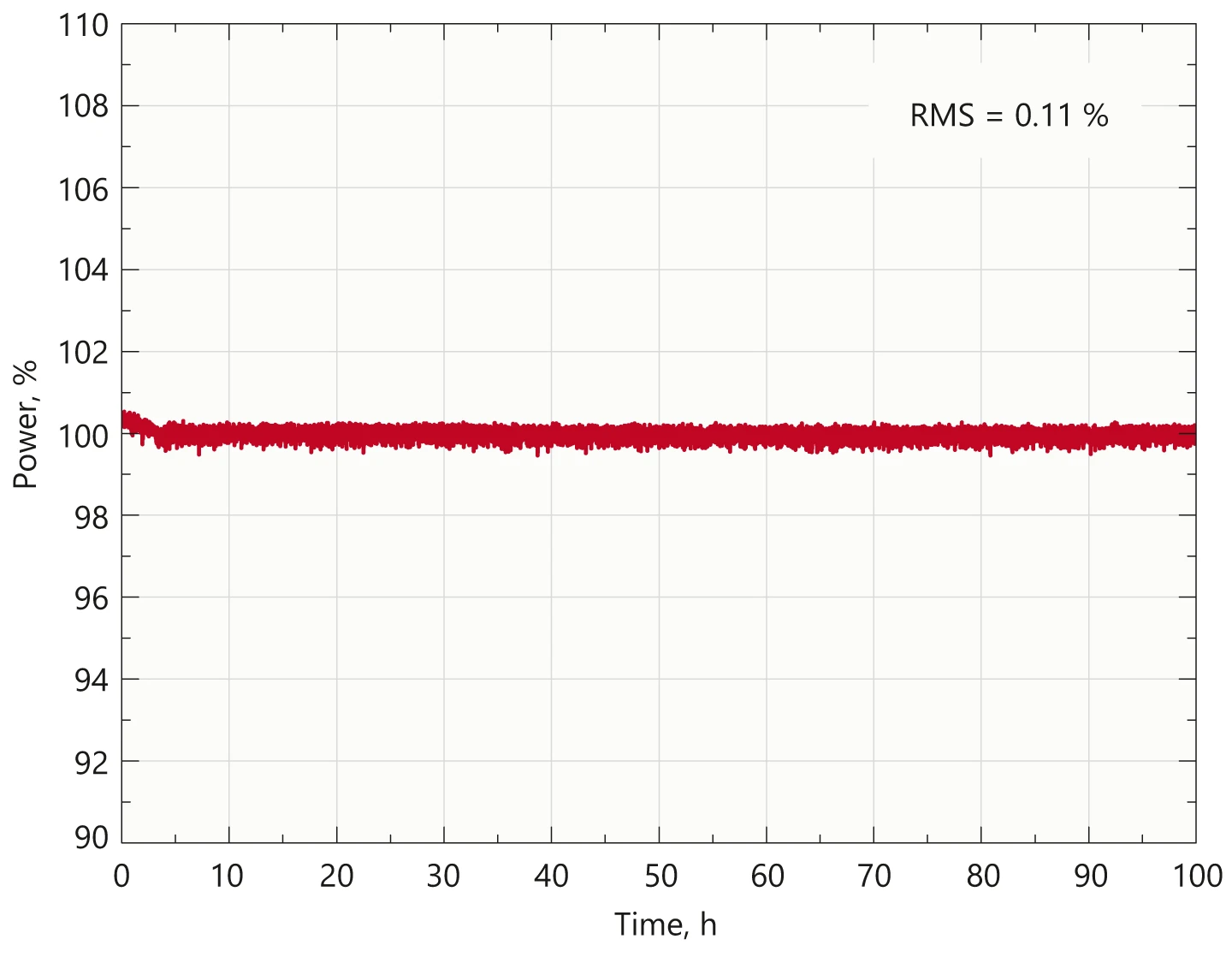
Typical long term average power stability of FemtoLux 50 laser at 1030 nm under constant environmental conditions.
Typical dependence of output power and pulse energy of FemtoLux HE laser at 1030 nm on pulse repetition rate.

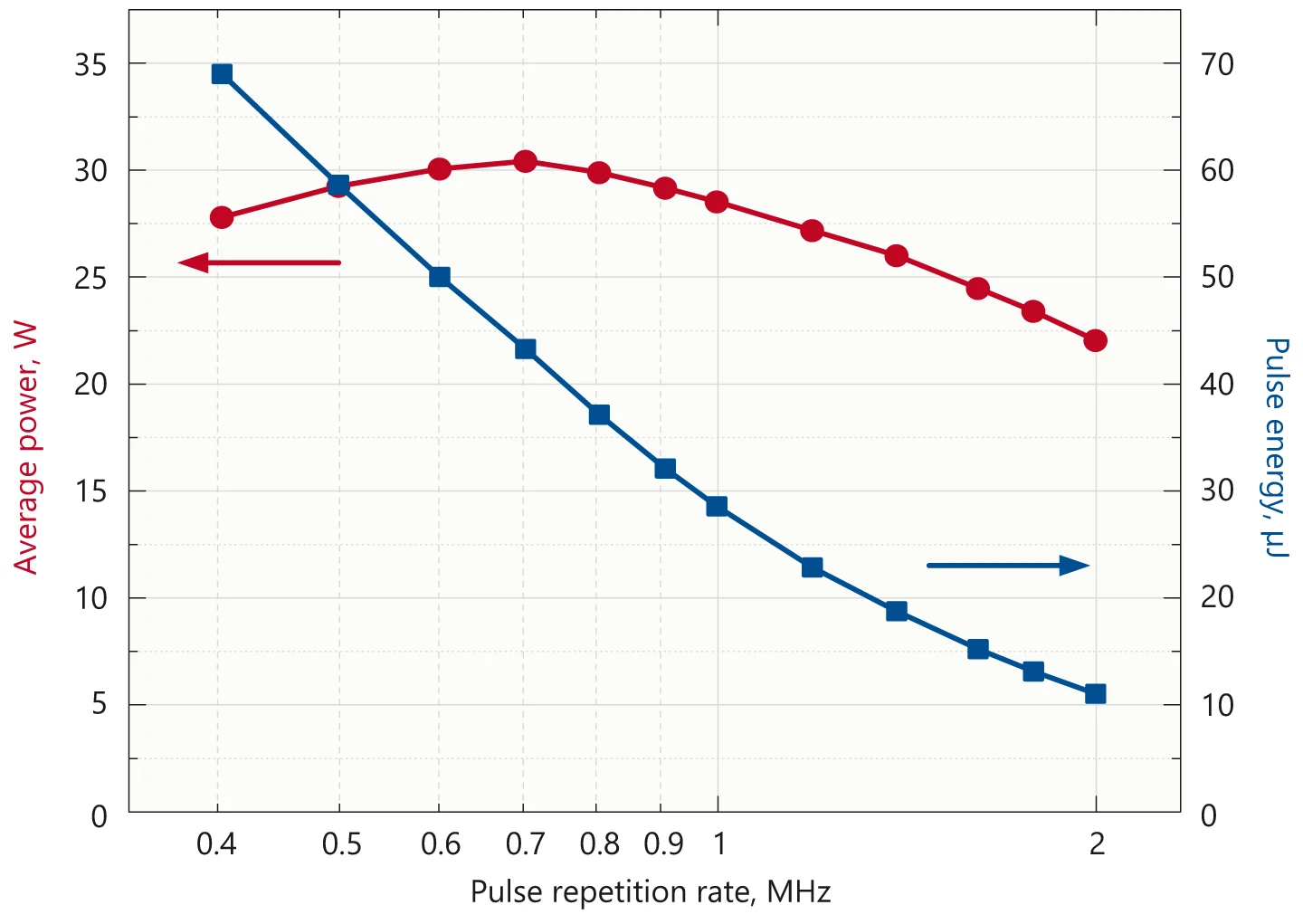
Typical dependence of output power and pulse energy of FemtoLux 30 laser at 1030 nm on pulse repetition rate.

Typical dependence of output power and pulse energy of FemtoLux 30 laser at 515 nm on pulse repetition rate.

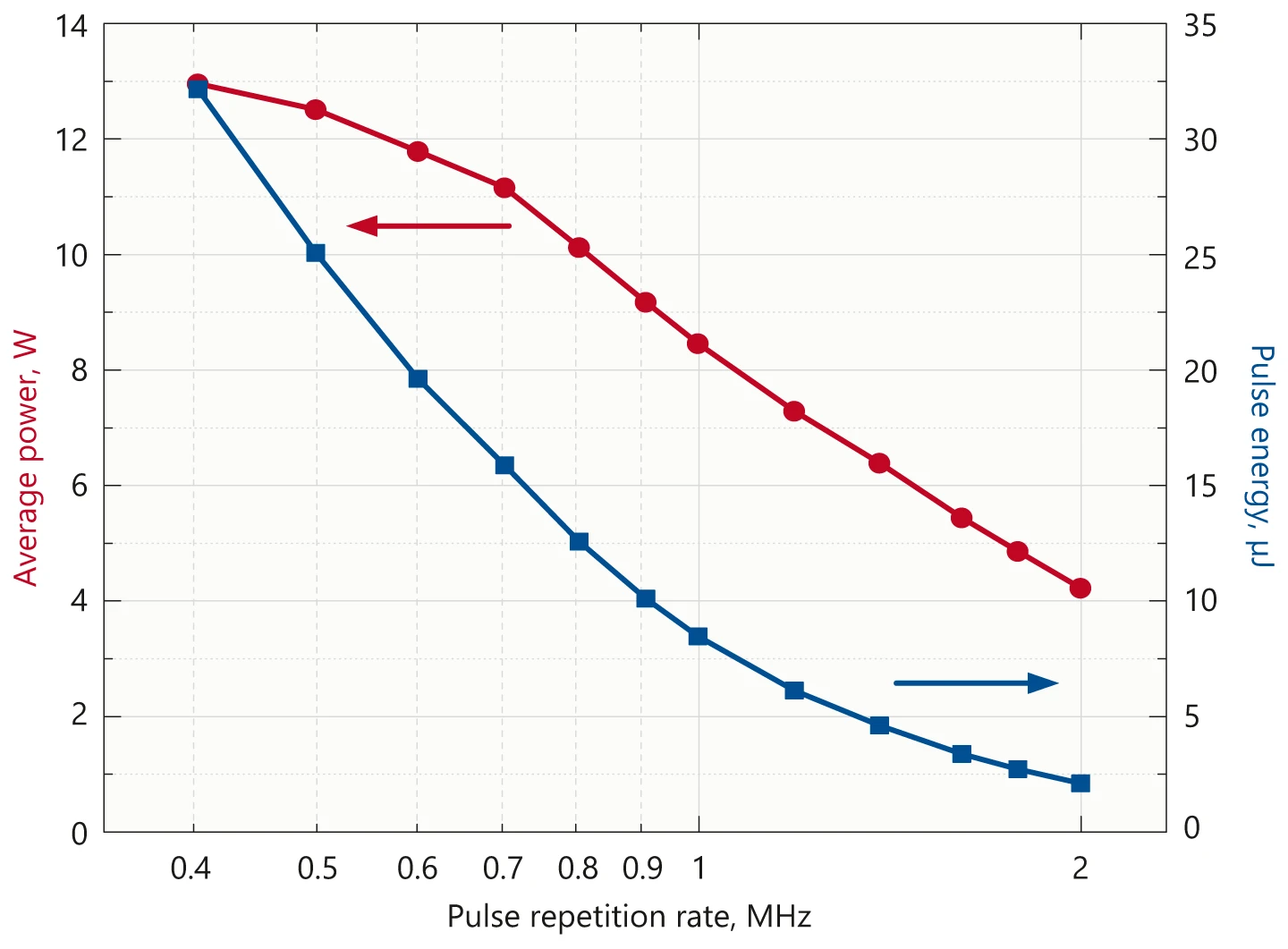
Typical dependence of output power and pulse energy of FemtoLux 30 laser at 343 nm on pulse repetition rate.

Typical FemtoLux 30 laser output pulse autocorrelation function at 1030 nm.

Typical M² measurement of FemtoLux 30 laser at 1030 nm.

Typical pulse-to-pulse energy stability of FemtoLux 30 laser at 200 kHz.
Over 30 000 pulses. RMS was calculated by using a set of mean values of 10 consecutive laser shots.
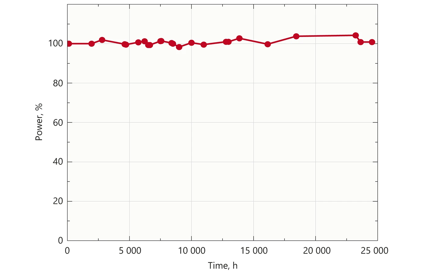
Long-term average power stability of the FemtoLux 30 laser at 1030 nm.
Under constant environmental conditions over an extended duration of 25,000 hours.

Typical long term average power stability of FemtoLux 30 laser at 1030 nm.
Under constant environmental conditions.

Typical beam direction stability of FemtoLux 30.
Under harsh environmental conditions.

Average output power dependance of FemtoLux 30 laser on ambient temperature at 1030 nm.
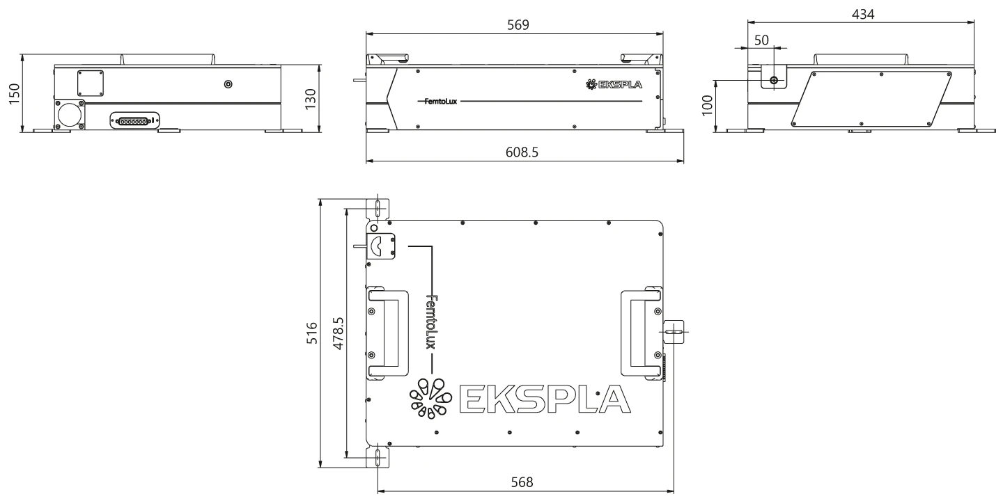
FemtoLux laser head outline drawing.
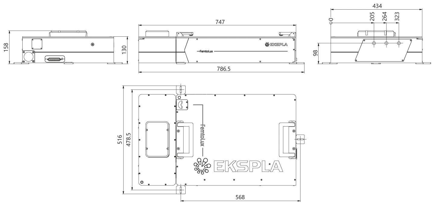
FemtoLux with harmonics module. Laser head outline drawing.
Femtosecond industrial laser FemtoLux with harmonics module.
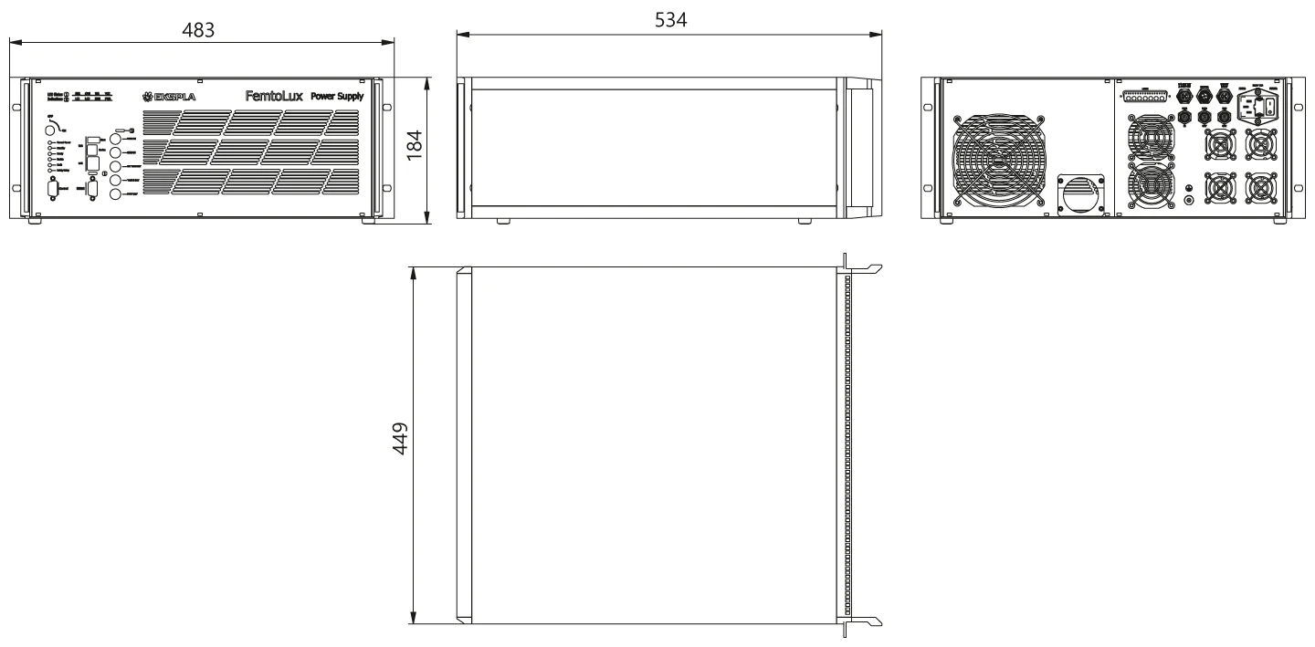
Power supply outline drawing.
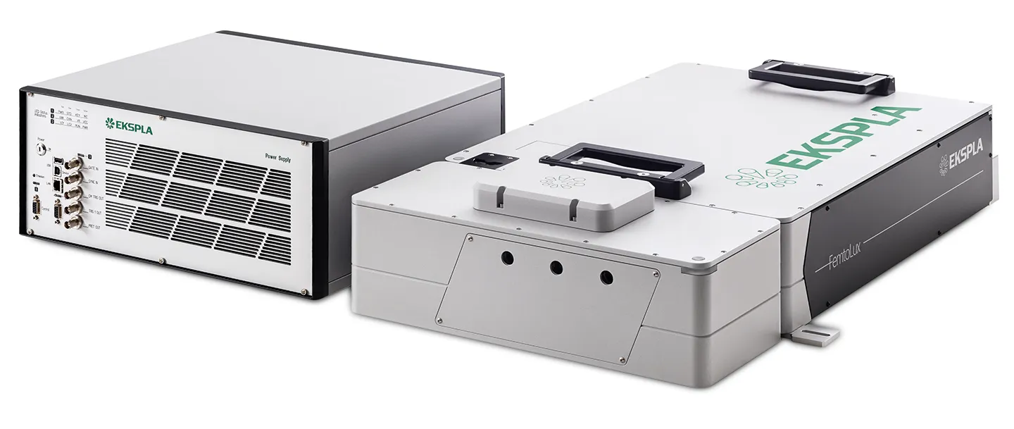
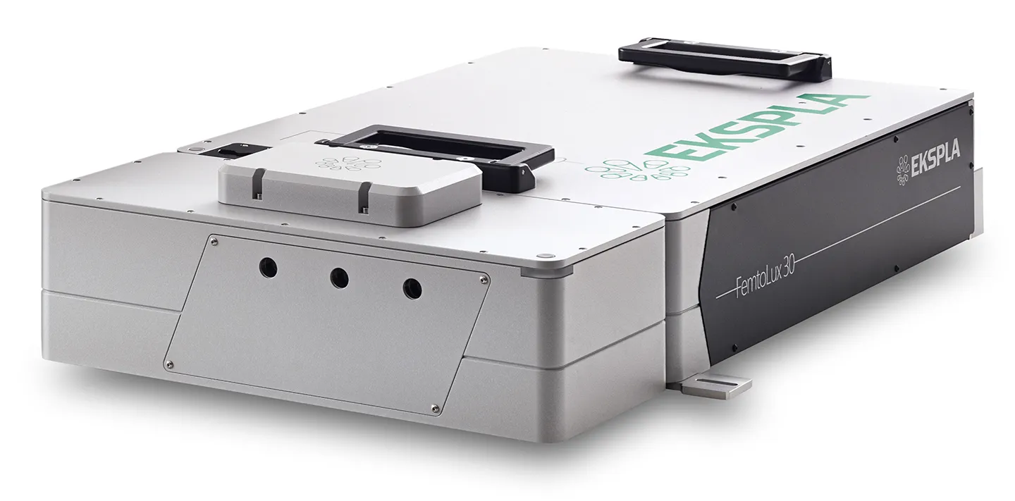
FemtoLux with harmonics module and power supply.
Ekspla Control Application is a software tool intended for day-to-day routine operation control. It is used to control the laser in API level through LAN or RS-232 communication types, the control capabilities are stored in the laser system itself, software is self-adaptive to the system, one application can be used with multiple systems and can run on different platforms – be it Windows, Linux or others using REST API commands.
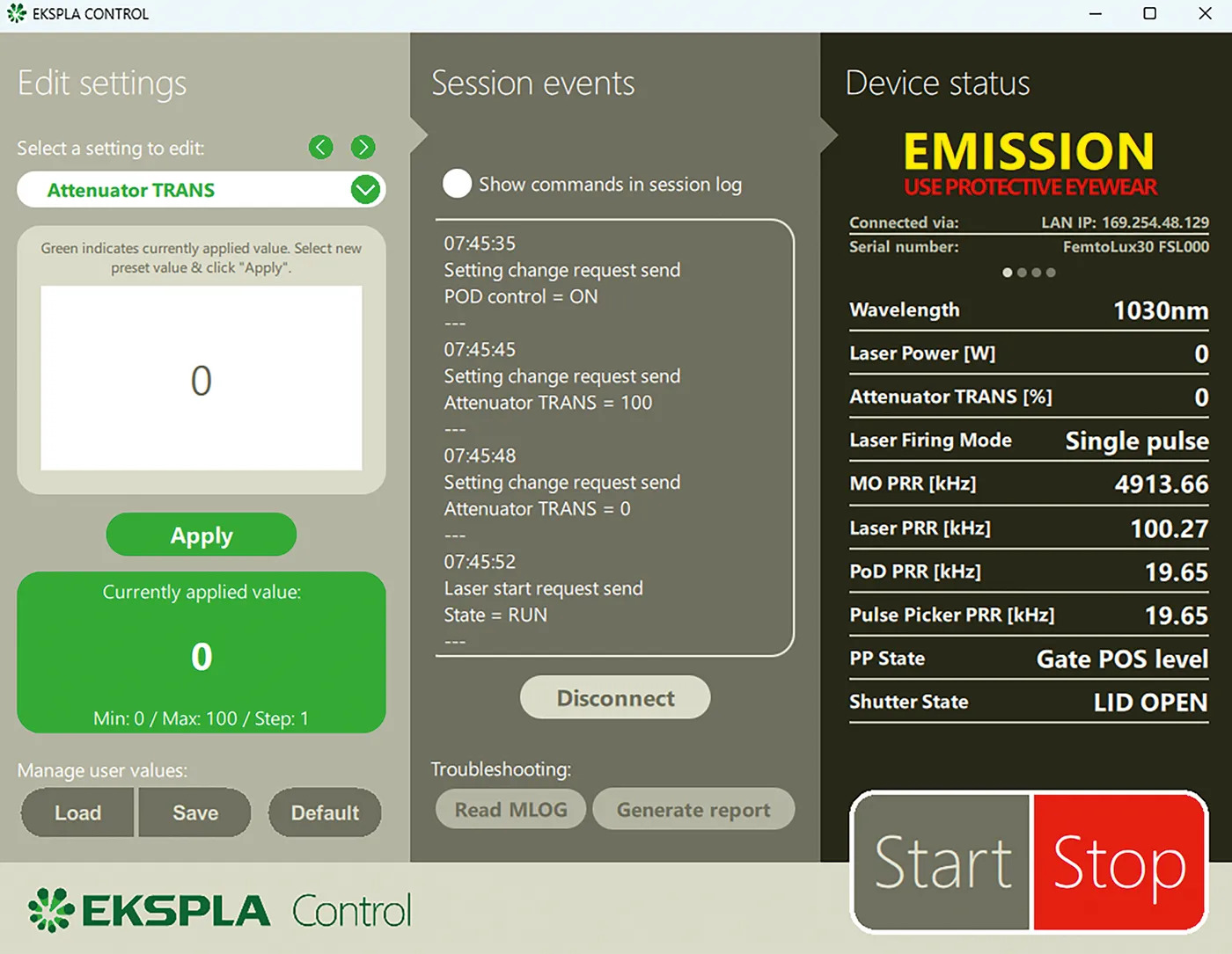
Laser control application.