Selective Surface Activation Induced by Laser (SSAIL)
SSAIL (Selective Surface Activation Induced by Laser) is a technology developed by the Center for Physical Sciences and Technology (FTMC) and Akoneer for writing electronic circuits directly onto dielectric surfaces. The process runs in three steps: an ultra-short pulse laser modifies the surface along the circuit pattern, the modified areas are chemically activated, and electroless plating then deposits copper only where the laser has written. Trace widths go down to 1 µm, and the process works on PC/ABS, PMMA, PET, FR-4, Al2O3 ceramic, fused silica, silicon and other materials.
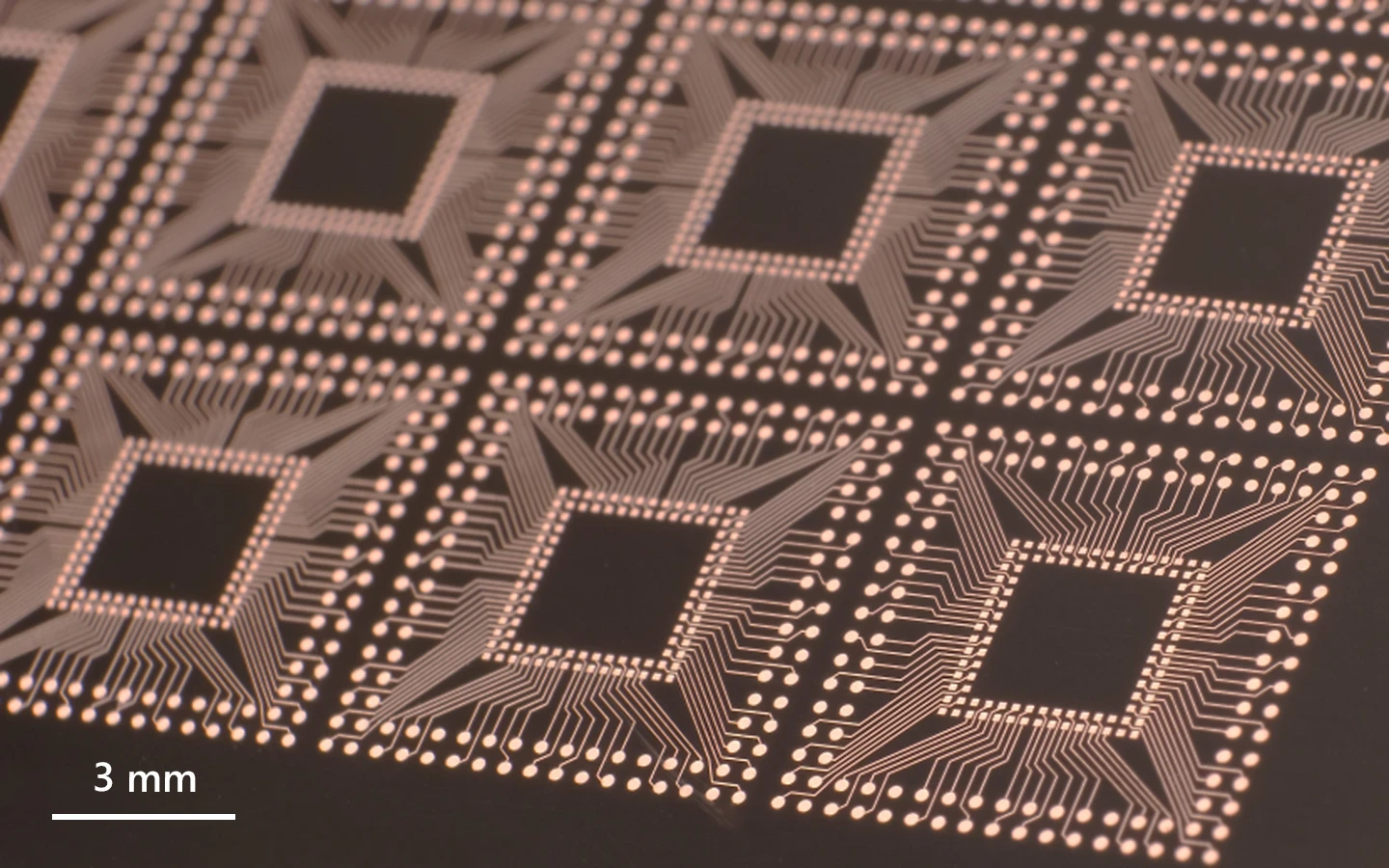
Copper circuit patterns on polyimide (PI).
Courtesy of Akoneer.
Manufacturing examples
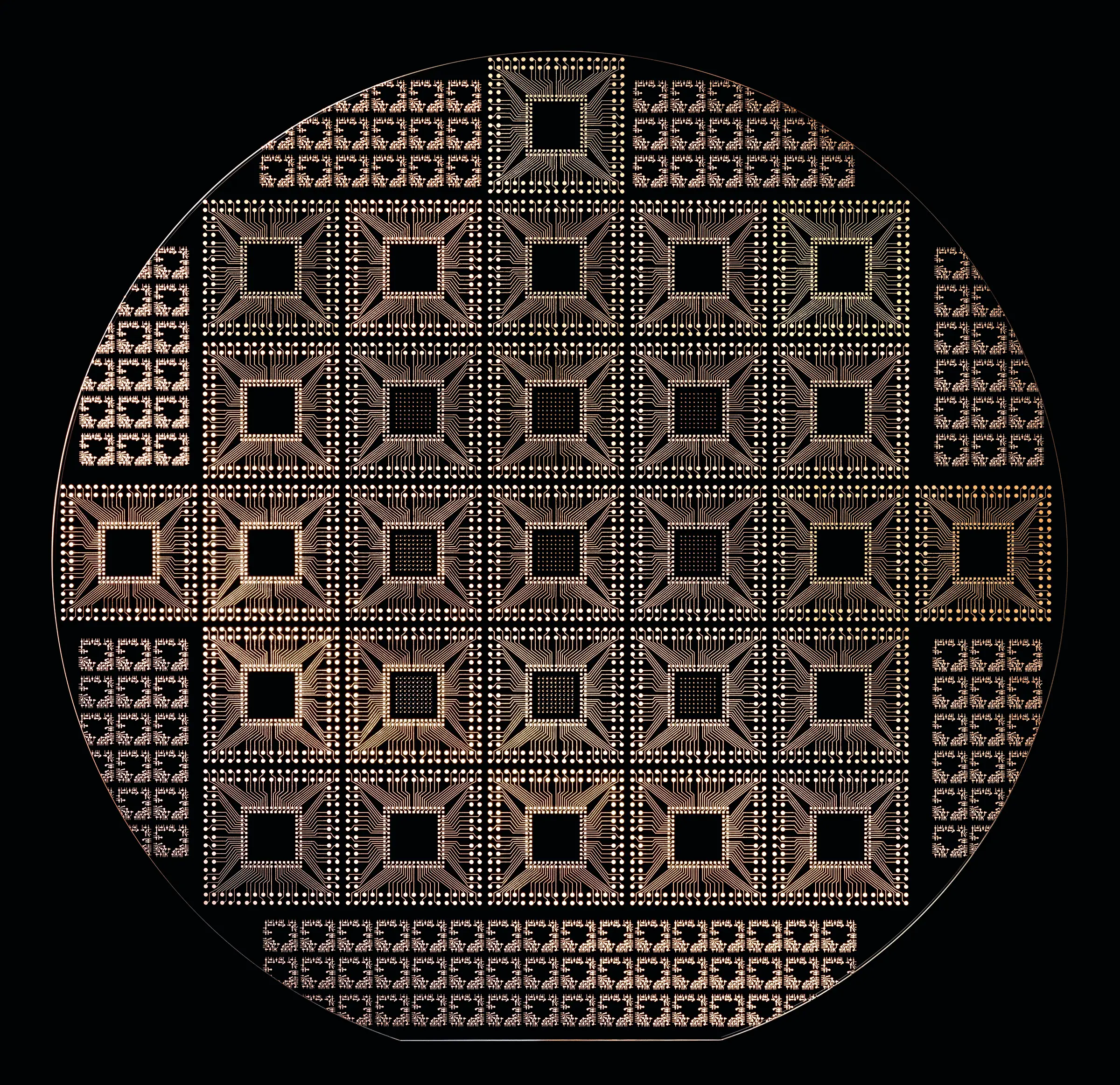
Copper circuit patterns across a full glass wafer.
Courtesy of Akoneer.

Dotted copper patterns on transparent glass.
Courtesy of Akoneer.
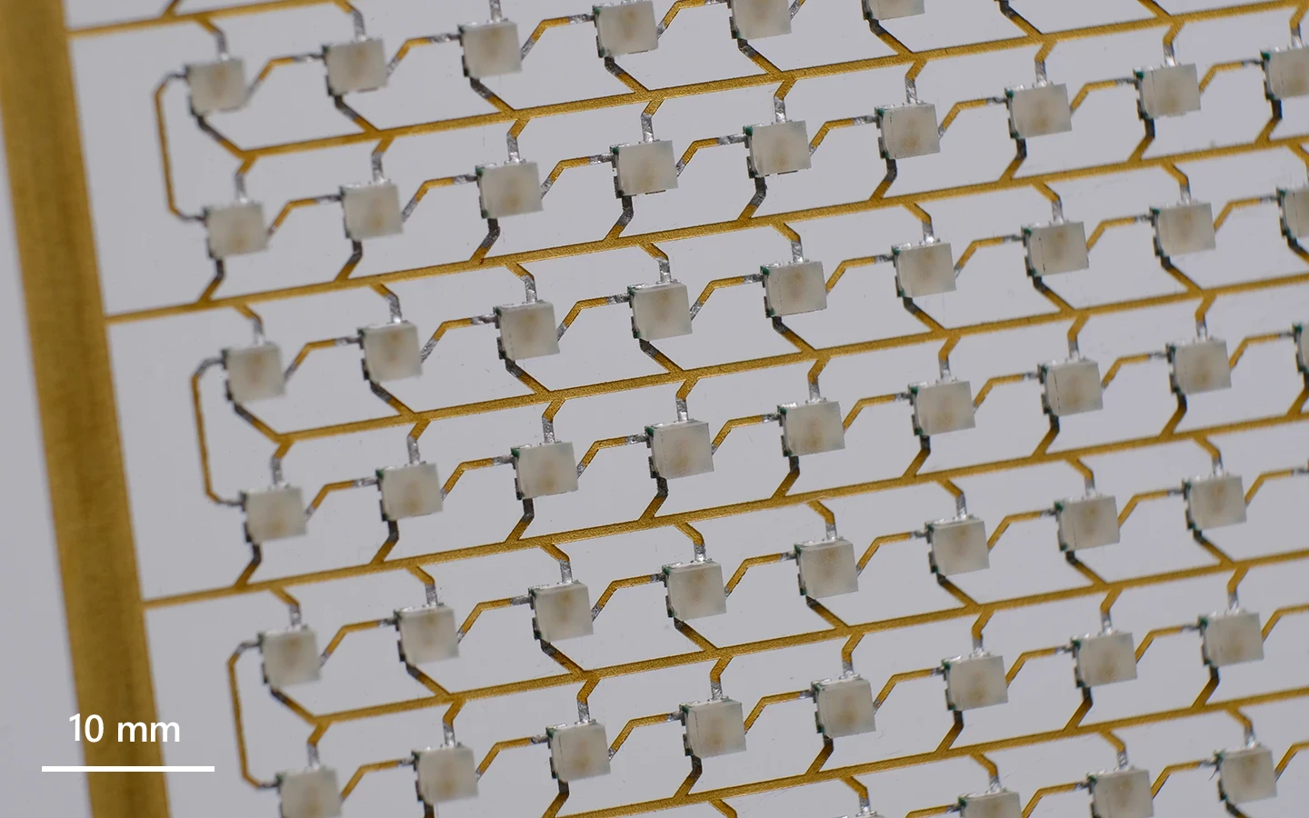
LEDs mounted on SSAIL-written circuits on glass.
Courtesy of Akoneer.

Copper traces on the curved surfaces of a molded 3D part.
Courtesy of Akoneer.

Transparent LED display demonstrator on PA4T.
Courtesy of Akoneer.