Femtosecond laser cutting of FZ-Si wafer
The production of customized optoelectronic devices often calls for silicon chips in specific shapes. Mechanical dicing is poorly suited to them: silicon cleaves along its crystallographic directions, which restricts the achievable shapes and leaves little control over the process. Femtosecond lasers cut smaller features with higher resolution and better processing efficiency than laser sources with longer pulses.
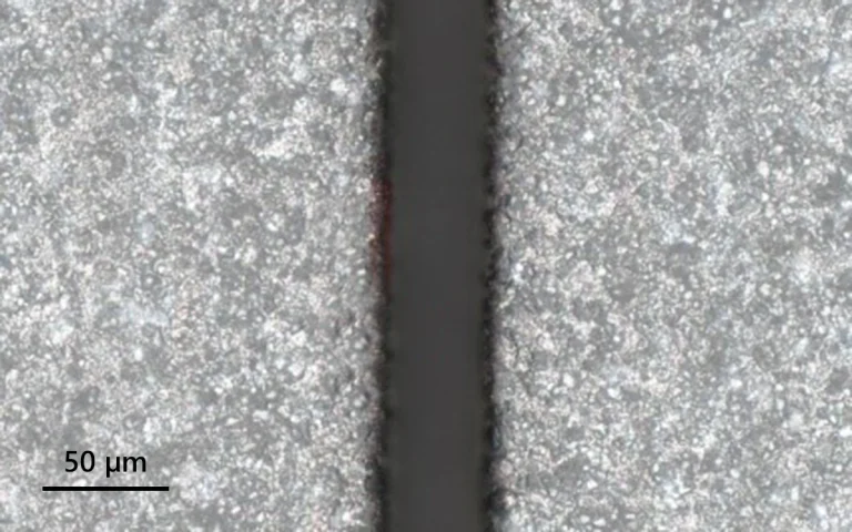
A float-zone silicon wafer (FZ-Si (100), 0.4 mm thick) was cut with a FemtoLux laser. Processing quality was high: a low heat-affected zone, no damage on the bottom surface, and curved contours that mechanical dicing cannot follow, as in the example below.
Manufacturing examples

Cutting of FZ-Si wafer.
Courtesy of FTMC.

Microscope image of processed FZ-Si wafer edge.
Courtesy of FTMC.