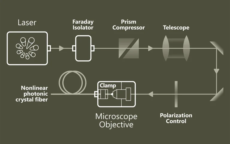
Time-resolved photoconductivity
Time-resolved photoconductivity (TRMC) are key techniques used to perform the contactless determination of carrier density, transport, trapping, and recombination parameters in charge transport materials such as organic semiconductors and dyes, inorganic semiconductors, and metal-insulator composites, which find use in conductive inks, thin-film transistors, light-emitting diodes, photocatalysts, and photovoltaics.
The behavior of photoconductivity with photon energy, light intensity and temperature, and its time evolution and frequency dependence, can reveal a great deal about carrier generation, transport and recombination processes. Many of these processes now have a sound theoretical basis and so it is possible, with due caution, to use photoconductivity as a diagnostic tool in the study of new electronic materials and devices.

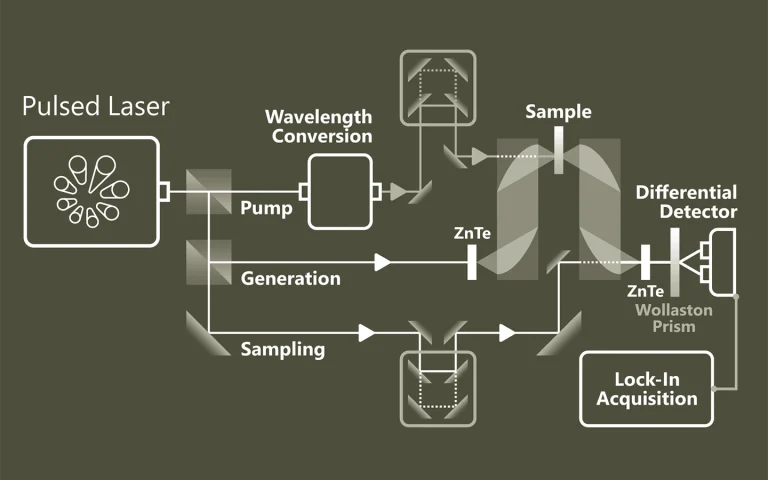
Principle of Time-Resolved Photoconductivity.